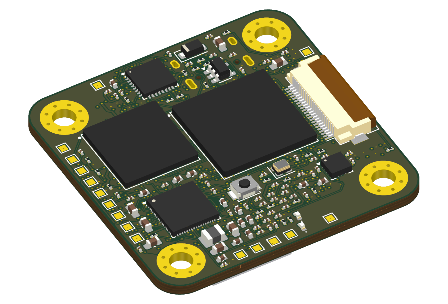
3D model
Drag to rotate, scroll to zoom. The processor, memory, eMMC, USB-C connector, microSD socket and one crystal use simplified block bodies of the correct outline; every other part uses its real package model.
Downloads: STEP for mechanical CAD, GLB for viewers, and a detailed GLB (large) that also includes copper, solder mask and silkscreen.
Specifications
| Item | Detail |
|---|---|
| Size | 39.5 × 39.5 mm, four M3 mounting holes |
| Layers | 8 (top, ground, signal + 1.8 V, signal, power, signal, ground + NPU rail, bottom) |
| Processor | Rockchip RV1126, 409-ball 0.65 mm pitch |
| Memory | LPDDR3 1 GB, 178-ball |
| Storage | eMMC 5.1 (153-ball) and microSD socket |
| Power | 5 V in over USB-C; RK809-2 power management IC plus one SY8089 buck regulator for the logic rail |
| Cameras | Two 22-pin 0.5 mm FFC connectors: one 4-lane MIPI CSI, one 2-lane MIPI CSI |
| Video out | Analog CVBS through an ADV7391 encoder |
| Sensors | ICM-20602 IMU (SPI), BMP280 barometer (I²C) |
| I/O on test pads | Debug UART, two more UARTs, four PWM, I²C, USB host, CVBS, 5 V and 3.3 V |
| Parts | 258 footprints, both sides populated; passives mostly 0201 and 0402 |
| Design rules | 0.09 mm track and gap, 0.35 mm via with 0.15 mm drill, through vias only, 41 vias in BGA pads |
| Tools | KiCad 10 |
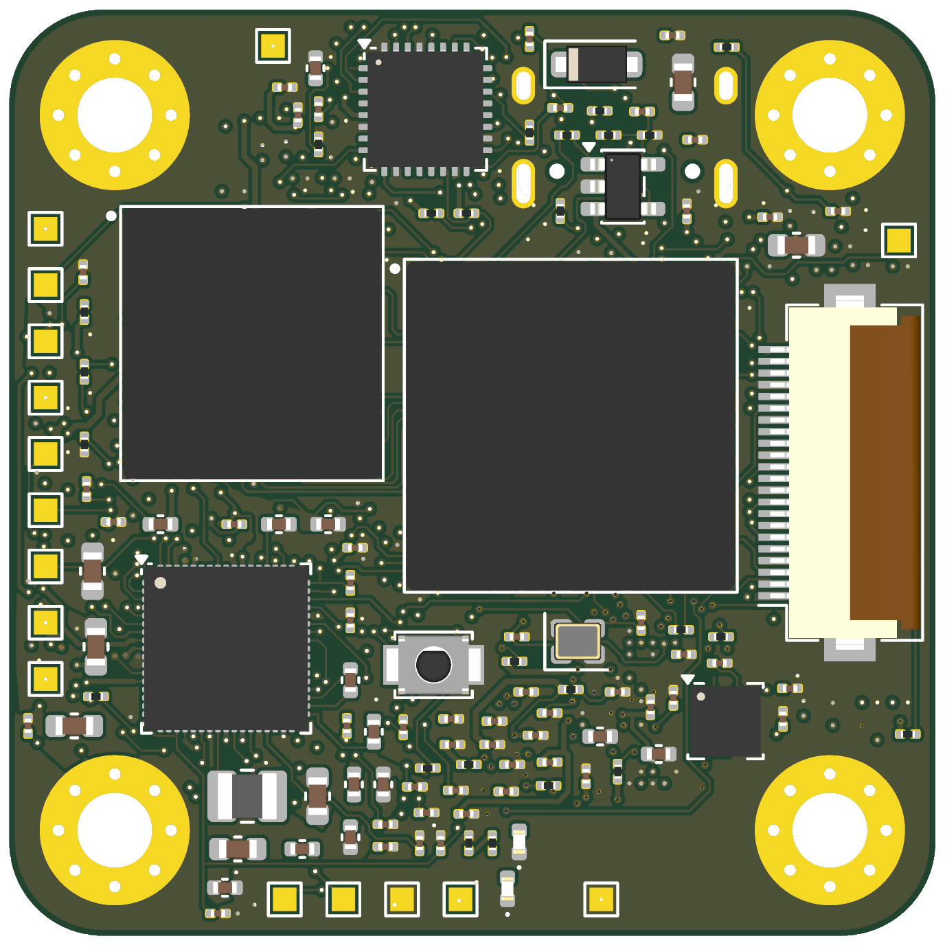
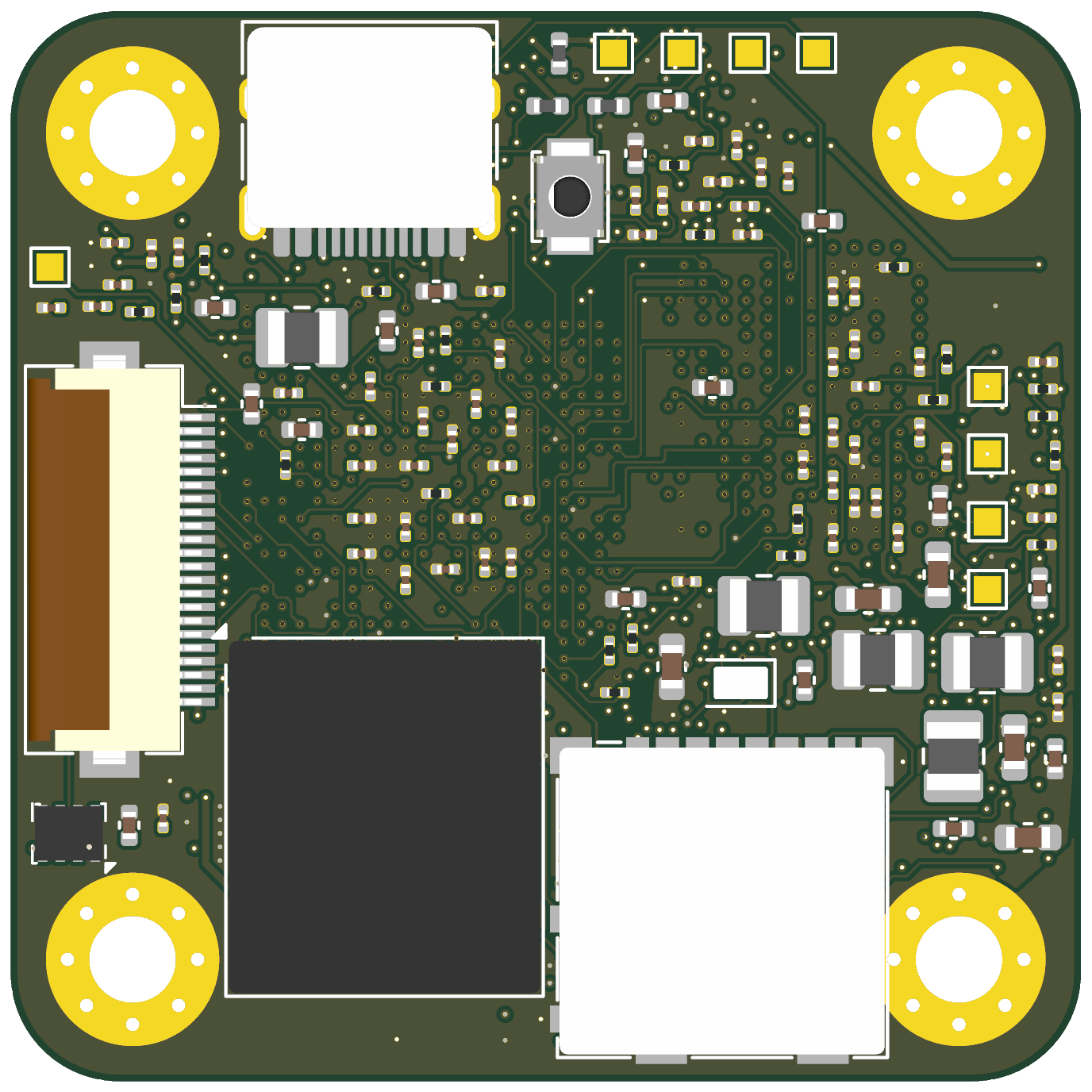
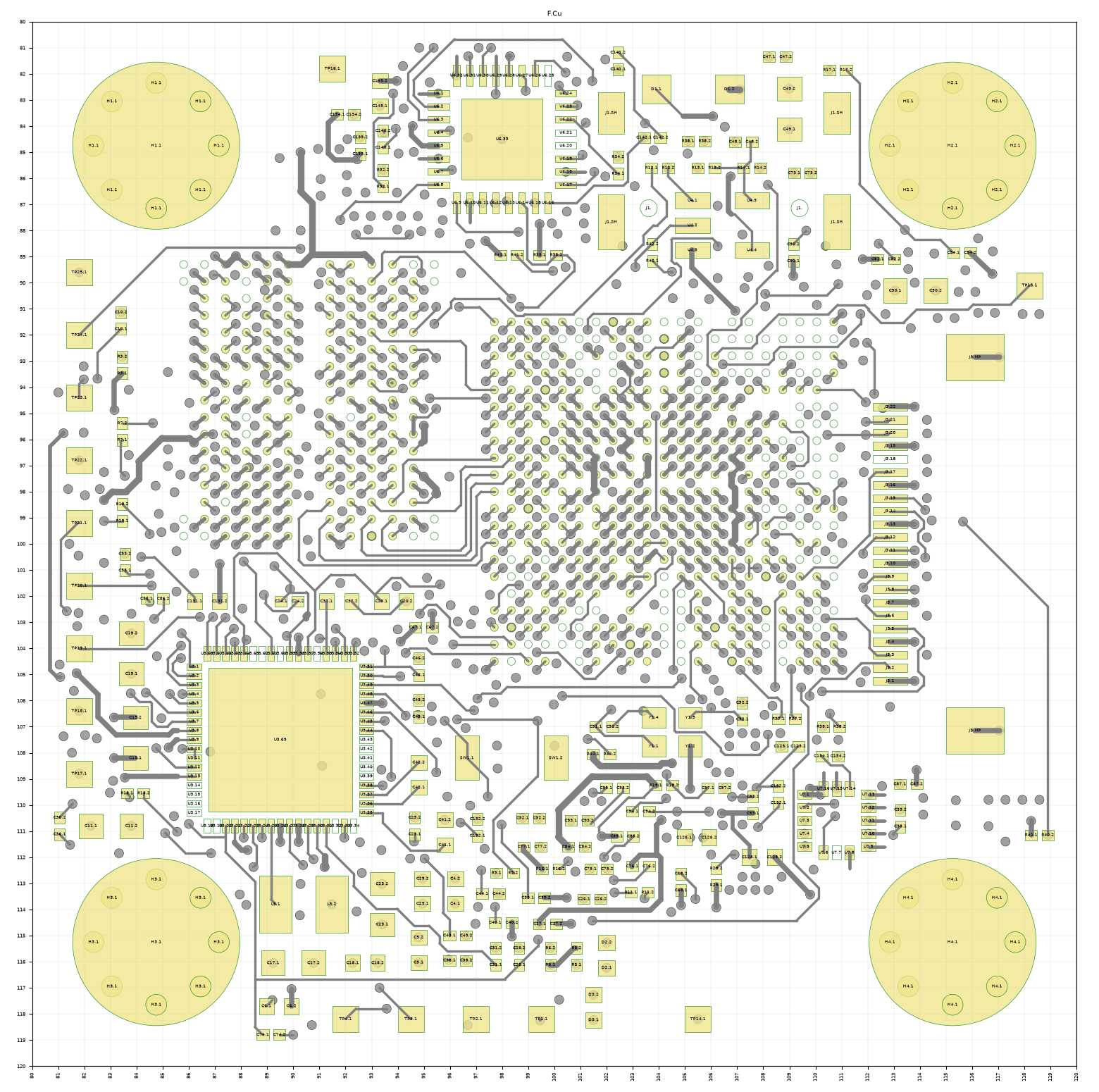
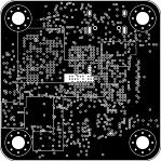
Renders
Downloads
ZIP · 1.4 MB Fabrication packGerbers, drill file, BOM and pick-and-place positions.
ZIP · 1.0 MB Gerbers onlyFlat ZIP ready to upload to a board house.
ZIP · 1.0 MB SchematicAll sheets as one PDF.
PDF · 0.6 MB Bill of materialsReference, value and footprint for every part.
CSV 3D model, STEPBoard with part bodies for mechanical CAD.
STEP 3D model, GLBSame model for web and 3D viewers.
GLB Generator scriptsThe Python that built the schematic, placement, routing and planes.
ZIP · 0.1 MB
How to use it
1. Open and inspect the design
- Install KiCad 10.
- Unzip the KiCad project and open
vision-rv1126.kicad_pro. The custom symbols and footprints load from the bundledlibfolder. - Open the board and run Inspect → Design Rules Checker. Expect no clearance or short errors, one unconnected ground ball and ten warnings; see Known issues.
- After any edit, press B to refill the zones before re-running the check. The plane layers depend on the project's 0.2 mm hole clearance rule being loaded.
2. Order bare boards
The fabrication pack was prepared with JLCPCB's published limits in mind, but it has not been through any manufacturer's own check. Upload the Gerber ZIP to their design review first and expect questions.
| Setting | Value |
|---|---|
| Layers | 8 |
| Size | 39.5 × 39.5 mm |
| Minimum track / gap | 0.09 mm / 0.09 mm |
| Minimum drill | 0.15 mm, via pad 0.35 mm |
| Via process | Filled and capped (the design has vias in BGA pads) |
| Surface finish | ENIG, for the 0.5 mm and 0.65 mm pitch BGAs |
| Impedance control | Not specified in the design; tracks are one uniform width |
3. Assemble
- Use
bom.csvandpositions.csvfrom the fabrication pack. Parts sit on both sides. - The three BGAs and the 0201 passives need stencil printing and reflow; this is not a hand-soldering board.
- The BOM lists values and footprints, not manufacturer part numbers. Choose and check exact parts before ordering, in particular the LPDDR3 and eMMC against the footprints.
4. First power-up
None of this has been done on real hardware; it is the sequence the design intends.
- Check for shorts between 5 V, 3.3 V, 1.8 V, the core rails and ground before applying power.
- Power from a current-limited 5 V supply through the USB-C connector and measure the rails at their decoupling capacitors.
- Connect a 3.3 V serial adapter to the debug UART pads (TP8 transmit, TP9 receive, any ground pad).
- Hold BOOT while applying power to enter Rockchip's USB download mode, then load firmware over the same USB-C port with Rockchip's tools.
- Start with a low memory clock. The DDR tracks are not length-matched, so the memory may not train at full speed.
5. Rebuild from the scripts
The board was generated by Python scripts that drive KiCad's scripting interface. They are included for reference; paths inside them point at the original working folder and need adjusting.
hand.sh        apply routes → build zones → refill → run DRC
plan.py        hand-planned DDR routing
maze.py        rule-checked path finder for all other nets
route.py       power and ground plane regions
lengths.py     DDR length report
Connectors and test pads
| Reference | Function | Notes |
|---|---|---|
| J1 | USB-C | 5 V input and USB OTG data |
| J2 | microSD | Bottom side |
| J3 | Camera 0, 4-lane MIPI CSI | 22-pin 0.5 mm FFC, Raspberry Pi 22-pin pin order, 3.3 V on pin 22 |
| J4 | Camera 1, 2-lane MIPI CSI | 22-pin 0.5 mm FFC, bottom side |
| SW1 / SW2 | Reset / Boot | |
| D2 / D3 | Green / red LED | Activity and status |
Test pads
| Pad | Signal | Pad | Signal |
|---|---|---|---|
| TP1 | 5 V system | TP15 / TP16 | UART0 TX / RX |
| TP3 | Power-on key | TP17 | CVBS video out |
| TP4 – TP7 | PWM0 – PWM3 | TP19 / TP20 | USB host D+ / D− |
| TP8 / TP9 | Debug UART TX / RX | TP21 | 5 V |
| TP10 / TP11 | UART3 TX / RX | TP23 / TP24 | I²C3 SCL / SDA |
| TP2, 12 – 14, 18, 22 | Ground | TP25 | 3.3 V |
Design notes
- Schematic. The processor, memory and power sections follow Rockchip's RV1126 reference design: LPDDR3 data-bit order, address and control mapping, and the RK809-2 rail assignment were checked against it. Passive values, strap pins and the peripherals were not checked line by line.
- Memory routing. The 59 timing-critical LPDDR3 nets were planned by hand, lane by lane, between the processor and memory.
- Everything else. A purpose-written path finder routed the remaining nets with exact clearance checks, lifting and re-laying tracks when a pin was boxed in.
- Power. Core rails are fixed plane regions: memory supply, ARM and logic rails on the power layer, the NPU rail on part of the second ground layer, 3.3 V filling the rest. The 5 V trunk is 0.4 mm wide.
- Form factor. Board size, mounting holes and connector positions follow the StingBee Vision V1.4 onboard computer so it fits the same mounts. This is an independent design, not affiliated with or endorsed by StingBee, and it was not derived from their design files.
Known issues
| Issue | Detail |
|---|---|
| DDR lengths are not matched | Spread of 4 to 8 mm within each data byte and 16 mm across address and control lines; strobe pairs differ by up to 2.5 mm. The memory may only work at reduced speed. |
| Never checked by a manufacturer | 0.09 mm tracks, 0.15 mm drills, vias in BGA pads and plane webs of about 0.1 mm between vias are all at the edge of standard capability. |
| Supply currents not verified | The 5 V, buck output and 3.3 V system nets still have 0.09 mm sections near the power management IC, backed by patchy copper pours. No current or voltage-drop calculation was done. |
| 1.8 V distribution | Shares an inner layer with signals and is stitched together from many pieces by tracks. |
| One unconnected ground ball | Processor ball AA10, one of about a hundred ground balls. |
| Tight assembly spacing | The eMMC courtyard overlaps the microSD socket's and one camera connector's; four mounting-hole pads fall inside a courtyard. |
| No controlled impedance | USB, MIPI and DDR pairs are not routed as coupled, impedance-controlled pairs. |
| Decoupling placement | Several decoupling capacitors sit far from the chips they serve. |